InGaAs Image Sensors Market Opportunities Rise in Semiconductor Wafer Inspection and Quality Control
Introduction
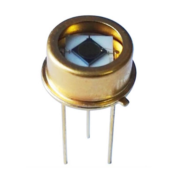
The demand for high-resolution, non-destructive inspection technologies in semiconductor production is rapidly elevating the relevance of the InGaAs Image Sensors Market. As chip geometries shrink and defects become increasingly microscopic and spectrally nuanced, shortwave infrared (SWIR) imaging with InGaAs sensors offers a powerful solution. These sensors provide unmatched capabilities for detecting internal irregularities, layer inconsistencies, and particle contamination—all without harming or contacting the wafer.
1. Why SWIR Imaging is Ideal for Semiconductor Inspection
Unlike visible light, SWIR penetrates silicon and other semiconductor materials to reveal subsurface structures. This enables:
-
Detection of voids, cracks, and delaminations
-
Inspection through packaging materials like epoxy and glass
-
Analysis of interconnects and embedded components
InGaAs sensors are especially suited to detect optical variations and material defects that traditional CCD or CMOS sensors cannot observe.
2. Front-End of Line (FEOL) Applications
InGaAs sensors play a vital role during the FEOL phase, where the transistor structures are created. Key uses include:
-
Substrate and epitaxial layer analysis
-
Oxide and metal film thickness uniformity checks
-
Monitoring of CMP (chemical mechanical polishing) quality
With SWIR imaging, process engineers can reduce defect escape rates, improve line yields, and optimize etching or deposition parameters.
3. Back-End of Line (BEOL) and Packaging Inspections
During BEOL processing, where interconnects and passivation layers are added, InGaAs image sensors help:
-
Evaluate wire bonding integrity
-
Detect moisture ingress under protective layers
-
Inspect through transparent encapsulants
Advanced packaging technologies such as 3D-IC, fan-out WLP, and chiplets benefit significantly from SWIR inspection, especially when combined with AI-driven defect recognition.
4. Non-Destructive Testing and Yield Optimization
Traditional inspection methods like X-ray or ultrasonic testing are either invasive or limited in detail. In contrast, InGaAs-based SWIR imaging allows:
-
High-throughput scanning without sample damage
-
Reduced need for destructive cross-sectioning
-
Inline inspection for real-time process feedback
These capabilities are critical for fab operators aiming to reduce scrap rates and accelerate time-to-market.
5. Integration with Automated Optical Inspection (AOI) Systems
Modern AOI platforms now include InGaAs sensors to expand their inspection range. Benefits include:
-
Full wafer mapping using hyperspectral SWIR imaging
-
Real-time analytics with pattern recognition and defect classification
-
Multi-sensor fusion with thermal and visible-light cameras
This hybrid approach enhances the robustness of inspections across different process steps and wafer types.
6. Cleanroom Suitability and Calibration Advantages
InGaAs sensors are designed to perform within cleanroom environments. Their advantages include:
-
Minimal thermal drift for consistent measurement
-
Rugged, sealed housing resistant to contamination
-
Compatibility with robotic handling systems
These features allow seamless integration into existing inspection lines and automated wafer handling stations.
7. Cost vs. Capability Trade-Off
While InGaAs sensors traditionally come at a premium, the ROI in semiconductor fabs is clear:
-
Reduced rework and rejection rates
-
Improved detection accuracy on advanced nodes
-
Shortened inspection cycles
As prices decline and foundries adopt more advanced process nodes (e.g., 5nm, 3nm), the cost of deploying SWIR solutions becomes increasingly justifiable.
8. Global Market Activity and Supplier Landscape
Major semiconductor equipment makers are now integrating InGaAs modules into their inspection platforms. Global activity includes:
-
Asia-Pacific fabs investing in inline SWIR systems for wafer-level reliability testing
-
European R&D centers incorporating SWIR into failure analysis labs
-
U.S. toolmakers launching turnkey SWIR-based metrology platforms
This growing supplier ecosystem is also encouraging custom sensor design, tailored optics, and application-specific firmware to address niche inspection needs.
Conclusion: Advancing into Market Restraints and Bottlenecks
The opportunities for InGaAs image sensors in semiconductor inspection are vast, especially as fabs scale complexity and volume. However, the market still faces notable restraints, including cost barriers and supply chain limitations. The next article will delve into these InGaAs market restraints, examining the challenges inhibiting broader deployment and potential strategies to overcome them.
- Art
- Causes
- Crafts
- Dance
- Drinks
- Film
- Fitness
- Food
- Giochi
- Gardening
- Health
- Home
- Literature
- Music
- Networking
- Altre informazioni
- Party
- Religion
- Shopping
- Sports
- Theater
- Wellness
- Politics
- IT
- Relationship
- Blockchain
- NFT
- Crypto
- Fintech
- Automobile
- Faith
- Family
- Animals
- Travel
- Pets
- Coding
- Comedy
- Movie
- Gioco
- Computer